In this blog, we cover our recent datasheet, “Deliver Innovative Products Faster with Jama Connect for Consumer Electronics Development” – To download this asset, click HERE.
Deliver Innovative Products Faster with Jama Connect for Consumer Electronics Development
Consumer electronics markets are highly competitive, with pressure on companies to deliver new and improved products fast. Falling short of consumer and supply chain expectations relating to product features, performance, or quality can hurt company reputations with buyers and resellers in the marketplace. Failure to satisfy applicable safety and environmental regulations can lead to
product recalls and payments to consumers and government agencies.
To be successful, companies must be able to develop new or improved products quickly by efficiently managing customer, market, and regulatory requirements across product lines with multiple configurations to meet the needs of buyers and regulators around the world.
Jama Connect for Consumer Electronics Development helps companies reduce time to market in delivering innovative, quality, affordable products to avoid recalls and reengineering, and stay ahead of the competition, and meet customer expectations. It supports compliance with IEC 62368 consumer electronics and IEC 60730 home appliance global safety standards.
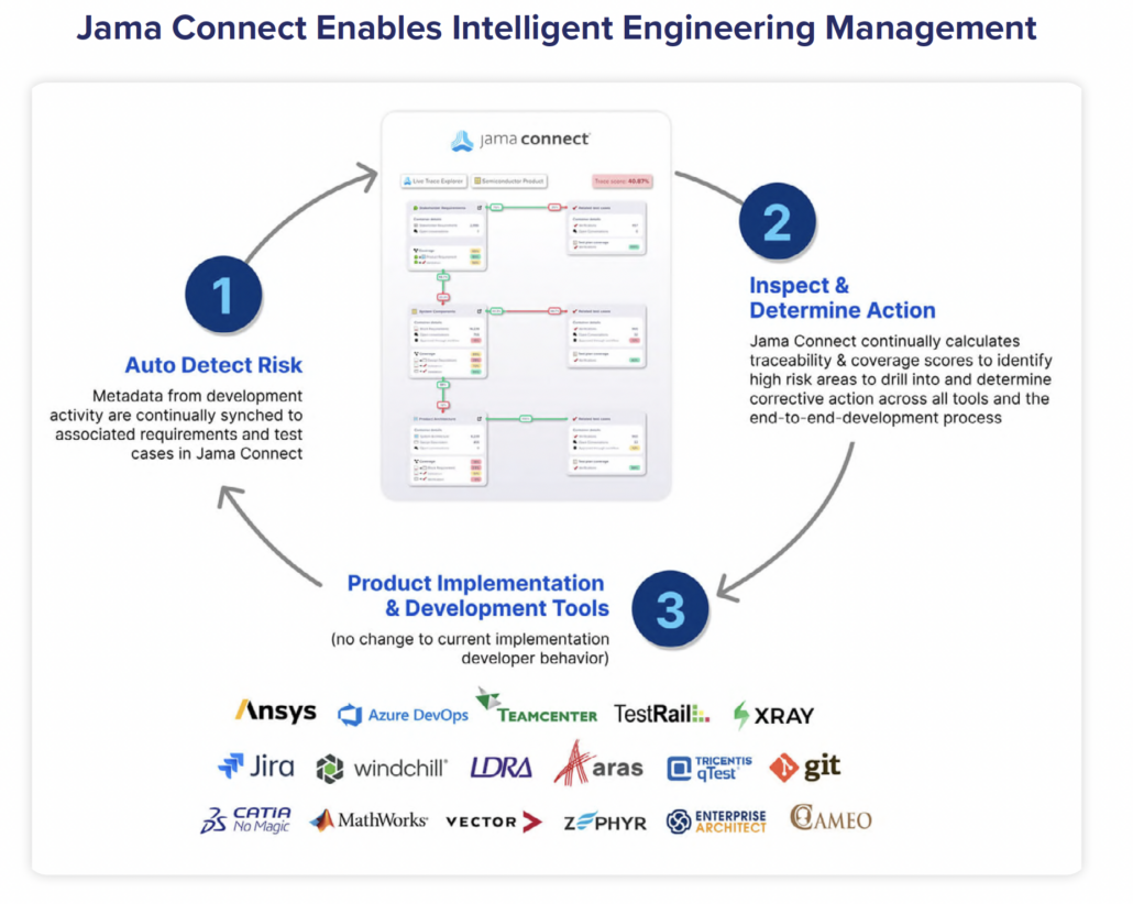
Guided, Measurable Product Development: Jama Connect’s intelligent engineering management enables significant reduction in re-engineering and product recalls by guiding the user through the end-to-end product development, automatically detecting gaps and risks across the entire engineering data, and automatically measuring the system and process completion.
AI Engineering Automation:Jama Connect Advisor’s™ AI will automate manual, day-to-day engineering tasks so that engineering can focus on innovation and problem-solving.
Digital Co-development Across the Supply Chain: With Jama Connect’s native co-development and engineering collaboration features, internal development and quality teams and external subcontractors and contract manufacturers can jointly define and develop products in the same source of truth in real time.
Apply Intelligence to Product Line Engineering: Efficiently manage requirements and tests shared by related products in libraries selectable based on the relevant configuration.
Streamline Safety and Cybersecurity Risk Analysis, Testing, and Compliance Reporting: Simplify adherence to applicable safety and cybersecurity regulations with pre-built requirements, automated test case generation for traceability, and templates for exporting compliance reports.
Jama Connect for Consumer Electronics Development Out-of-the-Box
Jama Software’s solution includes the following for developing integrated multidisciplinary consumer electronics products, subsystems, and software platforms:
Product, subsystem, and software development items
Product line engineering
Safety, risk, and cybersecurity regulation items
Co-development and digital thread process recommendations
Report templates
Organizations at the forefront of consumer electronics innovation recognize Jama Connect as the tool that provides a competitive advantage in the market by enabling the acceleration of development and bringing innovative products to market faster.
To learn more about managing your consumer electronics and home appliance requirements, tests, and risks more intelligently and efficiently with Jama Connect, visit jamasoftware.com
2026 Predictions for AECO: AI, Digital Twins, and the Path to Sustainable Transformation
As we step into 2026, the Architecture, Engineering, Construction, and Operations (AECO) industry is poised for a transformative leap. From the integration of AI and digital twins to the adoption of robotics and advanced materials, the sector is embracing innovation to tackle its most pressing challenges: sustainability, efficiency, and collaboration in a hybrid world.
This year’s predictions explore how emerging technologies like generative design, predictive analytics, and automation are reshaping the project lifecycle. We’ll dive into the role of advanced digital tools in achieving net-zero goals, the growing importance of cybersecurity in a connected ecosystem, and the long-term trends that will define the industry for years to come.
In part six of this year’s predictions series, we bring these insights to life with perspectives from Jama Software’s own AECO experts: Joe Gould – Senior Account Executive, and Michelle Solis – Associate Solutions Architect, who share their vision for the future. From AI-driven decision-making to the rise of modular construction and lifecycle optimization, this piece highlights the innovations and strategies that will shape 2026 and beyond.
Curious to read leading thought leaders’ predictions for their industries in 2026 and beyond? Dive into each blog below and stay tuned for part 6, the finale of this year’s series:
What specific emerging technologies (e.g., AI, digital twins, generative design, robotics) do you believe will have the most transformative impact on the AECO industry in the next five years? How can firms prepare to adopt and integrate these technologies effectively?
Joe Gould: AI and Machine Learning will become foundational across the entire project lifecycle.
Design & Planning: AI accelerates generative design by evaluating thousands of options against constraints like cost, performance, and sustainability—helping teams reach optimized solutions faster.
Predictive Insights: By analyzing large datasets, AI can forecast risks, schedule impacts, cost overruns, and potential failures, enabling earlier and more informed decisions.
Workflow Automation: Routine tasks such as data entry, document review, and quantity takeoffs are increasingly automated, allowing teams to focus on higher-value, strategic work.
Digital Twins extend these capabilities into operations.
Operational Optimization: Real-time digital replicas of assets enable continuous monitoring and simulation, improving energy performance, asset utilization, and long-term operating costs.
Predictive Maintenance: Simulating asset behavior under different conditions helps identify issues before failure, reducing downtime and extending asset life.
Collaboration: A shared, real-time data environment ensures all stakeholders are aligned on the most current information throughout the asset lifecycle.
Robotics and Automation have been moving from experimentation to real jobsite adoption.
On-Site Execution: AI-enabled robotics handle repetitive and high-risk tasks with greater precision and safety.
Autonomous Equipment: Drones and self-operating machinery are increasingly used for surveying, inspections, and material movement, improving efficiency while reducing labor constraints.
Sustainability and Net-Zero Goals
With the AECO industry under increasing pressure to meet sustainability and net-zero targets, what role do you see advanced software, materials innovation, and digital tools playing in achieving these goals? Are there specific technologies or strategies you think will lead the way?
Gould: Important question! Advanced digital tools allow teams to understand and manage environmental impact early in the process, long before construction begins.
At the core is Building Information Modeling (BIM), which provides a data-rich model that supports ongoing analysis of energy performance, material use, and constructability as designs evolve. Energy modeling and simulation extend this by forecasting real-world performance early, allowing teams to optimize efficiency and integrate renewables before decisions are locked in.
AI and machine learning add another layer by analyzing large datasets to improve decision-making, optimize resources, and surface risks earlier. Generative design helps teams evaluate thousands of design options that balance sustainability, cost, and performance. Digital twins, fed by real-time sensor data, carry this forward into operations—enabling predictive maintenance, smarter energy management, and continuous performance optimization over the life of the asset.
Life-cycle assessment tools tie it all together by informing material choices based on embodied carbon and long-term environmental impact, not just upfront cost.
Materials innovation focuses on reducing embodied carbon and supporting a more circular approach to construction.
This includes a shift toward low-carbon materials such as mass timber, green steel, and advanced concrete alternatives, along with greater use of recycled and reusable content. High-performance insulation and composites further improve operational efficiency by reducing long-term energy demand while maintaining durability and performance.
The real impact comes from integrating these tools into a single, data-driven approach—connecting design, construction, and operations.
Key strategies:
Data-driven decarbonization, using reliable project data for transparent reporting and continuous optimization
Prefabrication and modular construction, reducing waste, emissions, and schedule risk
Circular design principles, enabling reuse and recovery at end of life
Predictive maintenance, extending asset life and reducing long-term operational waste
By aligning digital tools, materials innovation, and lifecycle thinking, the industry can move beyond incremental gains and make measurable progress toward net-zero and long-term sustainability goals.
As hybrid and remote work models continue to evolve, how do you see these changes impacting collaboration, innovation, and project delivery in the AECO industry? What tools or processes will be critical for maintaining efficiency and creativity?
Gould: Hybrid and remote work are reshaping AECO, driving efficiency, expanding access to talent, and accelerating digital adoption—but they require more discipline around how teams collaborate and deliver work.
Collaboration has shifted from informal to intentional. Cloud-based platforms, shared models, and virtual design reviews are now standard, enabling distributed teams to stay aligned without being co-located. Innovation hasn’t slowed—it’s evolved. Access to broader talent pools and increased automation of routine tasks allow teams to spend more time on higher-value problem-solving.
From a delivery standpoint, hybrid models often reduce cycle times and costs. Work continues across time zones, travel is minimized, and documentation improves because communication has to be clearer by default.
Success in this environment depends less on tools alone and more on how they’re used. Cloud BIM, collaboration platforms, and project management systems form the backbone, but clear communication norms, standardized workflows, and outcome-based accountability are what keep teams productive.
To me, the shift isn’t about where people work—it’s about building repeatable, digital-first processes that support speed, clarity, and consistent project outcomes.
AI and Automation
How do you foresee AI and machine learning shaping decision-making, risk management, and project optimization in AECO? What are the biggest challenges or limitations the industry might face in scaling these technologies to automate processes?
Michelle Solis: While AI itself will make an impact on AECO companies, one additional area where we will see impact is in building the infostructure to handle the increase of AI usage across all industries. This will mean more jobs, job sites, data centers, and projects.
Gould: AI and machine learning are shifting AECO from reactive to proactive. When applied well, they improve decision-making, surface risk earlier, and optimize how projects are planned, built, and operated.
AI helps teams make better decisions by analyzing large volumes of historical and real-time data—highlighting patterns and risks humans typically miss. Generative design accelerates this by evaluating thousands of options against constraints like cost, performance, and sustainability. On the risk side, predictive analytics and real-time monitoring help identify schedule, cost, and safety issues before they escalate. AI also drives operational gains through task automation, smarter maintenance planning, and more resilient supply chains.
The challenge isn’t the technology—it’s scaling it. Most AECO firms struggle with fragmented data, limited system integration, and inconsistent standards. There are also a real skills gap and natural resistance to changing long-standing workflows. Add in high upfront costs, unclear use cases, unclear ROI, and legitimate concerns around data privacy and accountability, and adoption slows quickly.
The opportunity is real, but success depends on getting the fundamentals right: clean data, integrated systems, clear ownership, and practical use cases that tie directly to project and business outcome
Responsible AI Adoption
As AI and machine learning become more integrated into AECO workflows, what challenges or considerations should companies be mindful of to ensure successful implementation? How can firms address these challenges while maximizing the benefits of these technologies?
Gould: AI adoption in AECO isn’t a technology problem—it’s a fundamentals problem. Success depends on data, people, and how firms manage change.
Most organizations struggle with fragmented data, legacy systems, and limited AI-ready skills. Add natural resistance to new workflows, unclear ROI, and concerns around data security and accountability, and progress stalls quickly.
The path forward is straightforward:
Get the data right: standardize, govern it, and make it accessible
Upskill teams: treat AI as a productivity multiplier, not a replacement
Start small: focus on high-impact pilots that prove value fast
Modernize platforms: move toward cloud-based, integrated systems
Keep humans in the loop: clear ownership, transparency, and oversight matter
Firms that focus on these basics will scale AI effectively—and turn experimentation into measurable business outcomes.
Data-Driven Project Management
With the growing emphasis on predictive analytics, real-time monitoring, and data-driven decision-making, what strategies would you recommend for AECO firms to better harness data for optimizing project outcomes and resource allocation?
Gould: To use data effectively, AECO firms need to focus less on dashboards and more on fundamentals: integrated systems, clean data, and teams that actually trust and use it.
That starts with moving off siloed tools and spreadsheets and into cloud-based, integrated platforms that create a single source of truth across design, delivery, and operations. Strong data governance—clear ownership, standards, and quality controls—is non-negotiable. Without clean, consistent data, analytics don’t matter.
From there, predictive analytics should be embedded directly into project workflows, not buried in reports. Tracking the right KPIs and using data to flag schedule, cost, safety, and resource risks early shifts teams from reactive to proactive.
Finally, this only works if people are brought along. Start small with high-impact use cases, involve field teams early, and invest in basic data literacy, so insights drive decisions—not just meetings.
What upcoming regulatory changes or compliance requirements do you anticipate having the biggest impact on the AECO industry in 2026? How can companies stay ahead of these changes?
Gould: The biggest regulatory shifts hitting AECO in 2026 will center on ESG (Environmental, Social, and Governance), energy performance, and digital risk. ESG reporting is moving from “nice to have” to mandatory, with climate disclosure requirements cascading through supply chains. Energy codes will continue tightening, pushing firms toward higher-performance, low-carbon, and “zero-ready” buildings. At the same time, increased use of AI and cloud platforms is driving new expectations around transparency, governance, and cybersecurity.
The firms that stay ahead won’t treat this as a compliance exercise. They’ll lean on digital platforms to track energy, carbon, and materials from design through operations, put clear AI and data governance in place, and strengthen cybersecurity practices as reporting requirements tighten. Just as important, they’ll build regulatory awareness into project planning early—before requirements show up as cost, schedule, or risk surprises.
Cybersecurity in AECO
As digital tools and connected systems become more prevalent in AECO, what role do you see cybersecurity playing in protecting sensitive project data and ensuring operational continuity? Are there specific threats or solutions companies should prioritize?
Solis: As digital tools, connected platforms, and AI become more embedded in AECO workflows, cybersecurity will play a critical role in protecting sensitive project data and maintaining operational continuity. With the growing use of AI, firms must clearly define what data can and cannot be shared with AI models, particularly when working with proprietary designs, client information, or critical infrastructure data.
Beyond data leakage, organizations also need to address risks such as AI hallucinations, bias, and model misuse, which can directly impact design decisions, safety, and compliance if left unchecked. To mitigate these risks, companies should prioritize strong access controls, data governance policies, employee training, and secure AI deployments. Establishing clear guidelines around AI use, along with continuous monitoring and validation of outputs, will be essential to ensuring both cybersecurity and trust in digital systems as adoption accelerates.
Future of Innovation
What is the most innovative trend, tool, or process you’ve seen in the AECO industry recently? How do you anticipate it influencing the industry in the coming years?
Solis: One of the most impactful trends I’ve seen recently is the increased focus on Requirements Management across rail and broader AECO organizations. While this shift is often driven by hard lessons such as losing a contract or discovering unmet requirements late in a project, it signals a growing recognition that informal or disconnected requirement processes are no longer sustainable for complex, regulated projects.
Gould: The most meaningful innovation in AECO is the convergence of AI, digital twins, and integrated platforms. Together, they’re turning projects into connected, data-driven systems that move teams from static modeling to prediction, automation, and lifecycle optimization.
At the center is the digital thread. Requirements are no longer buried in PDFs and spreadsheets—they’re connected directly to BIM, schedules, costs, and real-time performance data. AI continuously validates designs against requirements, flags deviations early, and maintains traceability from concept through operations. That shift alone reduces rework, misalignment, and late-stage surprises.
AI-powered digital twins then extend this into delivery and operations, keeping stakeholders aligned and enabling smarter, faster decisions. The result is leaner execution, better compliance, and assets that actually perform as intended—not just on day one, but over their full lifecycle.
Long-Term Trends
What trends or technologies do you think will still be shaping the AECO industry five years from now? Ten years? How can companies position themselves to remain competitive in the long term?
Solis: I don’t think there’s one technology specifically that will shape the AECO industry. Companies who make an effort to welcome new technologies and not go against them will see success. This industry doesn’t want to evolve, but it will.
Gould: Over the next 5–10 years, AECO will be defined by digital maturity and industrialization. AI, BIM, and digital twins will move from tools to core infrastructure, while sustainability and offsite construction become standard, not optional.
In the next five years, BIM becomes the project command center—fully cloud-based and connected to schedule, cost, and lifecycle data. AI is embedded in planning and design to surface risk early, optimize decisions, and improve predictability. Modular and offsite construction scale quickly as firms respond to labor constraints and schedule pressure. Sustainability shifts from “nice-to-have” to a requirement.
Hard to say but looking ten years out I would predict that digital twins manage assets end-to-end, robotics handle more field execution, and buildings operate as connected systems within smart cities. Design, construction, and operations blur into a continuous, data-driven lifecycle.
The firms that win will invest early in integrated platforms, clean data, and workforce upskilling. They’ll focus on collaboration, specialization, and strong technology partnerships—turning digital capability into real project outcomes, not just innovation theater.
2026 Predictions for Semiconductors: AI, Chiplets, and the Path to Sustainable Innovation
As we step into 2026, the semiconductor industry stands at the crossroads of unprecedented technological advancements and complex global challenges. From the rise of AI-driven chip design and heterogeneous integration to the growing emphasis on sustainability and geopolitical shifts, the sector is navigating a transformative era.
The next wave of innovation will be defined by breakthroughs in advanced lithography, chiplet architectures, and quantum computing, while sustainability efforts will reshape manufacturing processes to address energy efficiency, water usage, and materials recycling. At the same time, the industry faces critical hurdles, including talent shortages, supply chain realignments, and the need for robust cybersecurity measures.
In this year’s predictions series, we’ve gathered insights from leading semiconductor experts:
Together, they explore the trends and technologies shaping the future of semiconductors. From AI-driven automation and edge computing to the challenges of regulatory shifts and the promise of chiplet-based architectures, this piece highlights the innovations and strategies that will define 2026 and beyond.
Q: What emerging technologies (e.g., advanced lithography, AI-driven chip design, quantum computing, heterogeneous integration) will have the most transformative impact on the semiconductor industry in the next five years?
Simon Bennett: In the next five years, the semiconductor industry will continue to grow, almost doubling in size from today to $1Trillion by 2030. But to sustain that growth, the industry will go through some extreme changes and challenges. The first trend to note is actually due to a declining trend as Moore’s Law continues to slow. [Editor’s note: Moore’s law is the observation that the number of transistors in an integrated circuit (IC) doubles about every two years.]
Moore’s Law has driven the growth of the Semiconductor industry for many decades, but it is bumping up against the fundamental laws of physics. The economics of scaling to the next node are increasingly prohibitive and taking longer and longer to reach fruition.
Whilst keeping an eye on what is coming out of China, there will be some more mundane but equally challenging technology trends that are emerging and will become increasingly important in 2026 and beyond. These are AI driven design, and both chiplet and wafer scale designs (two opposite ends of the spectrum, but both an engineering reaction to the slowing of Moore’s Law).
Neil Stroud: Given the ever-increasing innovation around AI and its associated deployment, chip development is under continued pressure to keep up. This is applicable across all architectures, including Central Processing Units (CPUs), Graphics Processing Units (GPUs), and Neural Processing Units (NPUs). Naturally, continued optimization will happen around acceleration and emerging technologies like process node shrinks (advanced lithography), AI-driven chip design, and the chiplet approach (heterogeneous integration). Process node shrinks will contribute. However, the chiplet approach will also drive heterogeneity across architectures and nodes. All these factors will intimately impact the next generation of chip families for AI in the datacenter and at the edge.
2: Sustainability and Manufacturing Efficiency
Q: How do you see sustainability influencing semiconductor manufacturing, particularly in areas like energy efficiency, water usage, and materials recycling? What strategies will help the industry achieve greener fabrication processes?
Bennett: This is a great question, and right now, the elephant in the room. From Fabs to datacenters, the environmental impact is huge. Water consumption alone is a huge factor. Twenty years ago, visionary realtors quietly purchased acres of land close to a bountiful supply of water and close to a large data pipe. Those realtors are now wealthy, and the secret is out. Now the price of that land is at a premium. So, the investors behind the fabs and the datacenters are using government subsidies and their own funds to find alternative sources of energy and resources. Nuclear is making a comeback, driven in part by the energy demands of the datacenters. Municipal areas like Phoenix are making guarantees of plentiful water to companies to attract them to their region; that will put them in direct conflict with farmers in California.
Most of this is happening off the radar of the mainstream media, and the political arena is presented as a battle for the best jobs. The concern over the environmental impact is not yet front and center. Two events will likely happen to change this:
The AI bubble will inevitably burst. Just like in the early days of the internet, there will be market correction as reality catches up to expectation. Just like the internet bubble, this doesn’t mean that AI is not going to be a societal change; it just means the market got too overheated.
Unfortunately, there will be some kind of accident related to the overbuild of the infrastructure around Datacenters and Fabs. A dam will burst (Phoenix – see Roosevelt Dam), or a multibillion fab will be damaged by a natural disaster (see fault lines in Taiwan). These two events will raise awareness of environmental costs relating to sustainability and manufacturing efficiency.
In other words, in the next five years, we will be forced to take a pause, a breath, and truly measure the value vs the cost. This isn’t a bad thing. Our human history of technology transformations is punctuated with these pauses and resets. Usually for the better.
Steve Rush: Sustainability is hugely influential and important. Energy demand is forecasted to accelerate with new data centers and the demand for AI. Semiconductor companies need a system to help manage their sustainability requirements and, very importantly, validate them. Implementation to hit targets and balance, power, efficiency, and sustainability will be a series of trade-offs – semiconductor organizations will need a tool to trace all of this information and prove that they meet sustainability targets and goals.
Sarah Crary Gregory: While the semiconductor industry is obviously fiercely competitive, it can match that intensity with fierce collaboration on critical issues. Sustainability is probably the most prominent area where industry consortia such as the Semiconductor Climate Consortium bring companies together to tackle common problems. Initiatives to enable water reclamation, reduce emissions, and produce data quantifying the return on investment of sustainability practices will be more critical with the burden placed on these resources from the exponential expansion of AI. The semiconductor industry is highly interdependent, and nobody believes that there’s a way to get a competitive advantage by monopolizing natural resources. The way forward is through innovations that decrease resource consumption and minimize waste, and initiatives for water reclamation/”net zero” resource use will continue to be essential investments.
Stroud: I think there are two parts to this. Firstly, the environmental impact of actually building the chips in foundries. A huge amount of effort and investment has gone into sustainability in semiconductor manufacturing, including energy efficiency, water usage, and materials recycling. semiconductor manufacturing and materials. A great example of this is massive recycling of water used in fab processes, as well as optimizing processes and the associated chemicals used, including minimizing atmospheric emissions.
Secondly, there is the environmental impact related to the deployment of the device itself, as it consumes power and emits heat. Of course, the extreme example of this is the data center where huge racks of GPUs or CPUs are deployed, collectively consuming Megawatts of power to both power them and cool them. Again, huge investment is going into driving data center efficiency. One way to contribute is through chip design optimization to improve ‘performance per Watt.’ That is simply a measure of how much computing can be done for a given Watt of power. This optimization can happen through design and architecture efficiencies as well as process node shrinks. Ensuring the software stack is also developed to drive efficient use of the underlying hardware platform also has a fundamental role to play. It’s easy to see that these steps can have a profound positive impact on the environment caused by the global electronics footprint.
Q: How is AI accelerating innovation in semiconductor design, verification, testing, and manufacturing? What challenges must companies overcome to fully leverage AI-driven automation?
Bennett: Natural language and agentic AI will continue to show up across the tool chain. But expect some resistance from SOC design engineers, who, ironically, since they are at the epicenter of the AI revolution, are traditionally conservative and slow to adopt new methods. Verification is the most in need of help with AI-driven automation, since there just aren’t enough engineers on the planet to drive the verification needs of an SOC. (see salaries on Glassdoor). It’s been estimated that with the use of AI, a team of 3 expert verification engineers can do the work of 5 traditional verification engineers with limited use of AI, in 3 to 5x less time. This is a compelling message to an (open-minded – see below for a caveat) engineering VP struggling to find the resources to deliver a fully validated product on time. These engineers and the tools they use will be in high demand in the next five years.
Beyond design, AI will show up in yield and manufacturing analytics. The challenge of inventory and yield management in the era of disaggregated chiplet-based designs is magnified. It’s essential that all the chiplets deliver the yield and volume needed at the exact same time. The overall package is only as good as the weakest tile. This is an underserved opportunity within the big three EDA companies, and the packaging OEMS tend to jealously protect their homegrown investments in solving these challenges. Expect emerging startups to come forward as disruptors in this particular segment in 2026 and beyond.
Rush: Every company is looking for ways to utilize AI in their organization. AI can play an important role in managing traceability, especially from siloed systems that are isolated from one another. Agentic experiences that improve engineer productivity really are key. The main challenge that AI has in the semiconductor space, in particular, is adoption with the engineering team. AI experiences must improve engineering productivity; they must be accurate, and they cannot be an impediment to use. If AI-generated content is of questionable quality or if the AI experiences become too burdensome to use, AI initiatives risk dying on the vine.
4: Supply Chain and Geopolitical Shifts
Q: How are global supply chain realignments and geopolitical factors shaping semiconductor strategy? What can companies do to mitigate risk and ensure resilience in developing complex products on their own or with co-development partners?
Bennett: A global supply chain developed over the past thirty years has delivered $1T in cost savings. This $1T is now under serious threat as the world is a very different place compared to when this globally interconnected environment was first conceived. In the next five years, expect China to become more self-sufficient as it replicates every aspect of what it previously relied on from overseas, from EDA to IP to fab equipment. Expect to see semiconductor-based products from coffee machines to phones to servers to (even) EVs sourced almost exclusively from China with little to no reliance on anything beyond the shores of China. This will trigger protectionist measures in the US and the EU as they work to protect homegrown industries from what will become increasingly consumer appealing products from the Chinese factories.
A more optimistic view may be that the tensions ease as the US / EU recognize the need for open trade with China, and continue to see its designs realized in Chinese factories (but I’m not holding my breath). In semiconductors, companies will be most susceptible to this shift in China as they move to homegrown alternatives. As the geopolitics ramp up, the focus on Provenance in the West will become a C-suite / US Senate / EU Parliament level of attention. Knowing where every component or piece of code originates, its genealogy will become paramount. A counterforce will emerge where the information is “buried” as the realization hits that we can’t possibly trace the root of every bit of code, every nanometer of design. Companies will emerge with one of two unique value propositions: 1) we can audit your product and provide the provenance, 2) everything you use is contaminated; we are a new company, built cleanly from the ground up. Somehow, all three will survive – the traditional companies, the auditors, and the new “clean” companies. But there will be some very interesting mergers and acquisitions, mostly off the radar as these three entities re-align and learn to co-exist.
Rush: These days, you can basically count on major geopolitical news covering the semiconductor industry week in, week out. At the end of the day, co-development and partnerships are key. The semiconductor supply chain is mind-bogglingly complex. Adopting modern, more collaborative tooling is on the rise. Historically, the semiconductor industry has even been hesitant to adopt cloud-based solutions, and I’ve definitely seen a change in the last few years around this.
Stroud: Like many other segments, the semiconductor market tends to be cyclic, which leads to times of undersupply and oversupply. This is a complex problem to manage with many factors, including global supply chain realignments and geopolitical factors. Naturally, foundry capacity has a big role to play, and we seem to be in an investment phase right now with a number of fabs being built. This is a massive investment with a modern fab costing tens of billions of Dollars and taking multiple years from construction start to mass production. Communication and collaboration across the ecosystem also has a role to play, especially now that we are accelerating into the chiplet era, which can help mitigate risk and ensure resilience in developing complex products.
5: Chiplet and Heterogeneous Integration
Q: What role will chiplet architectures and heterogeneous integration play in addressing performance and scalability challenges? What technical and ecosystem hurdles must be overcome?
Bennett: Chiplets are essential to the continued growth of Semiconductors. Without chiplets, the forecast CAGR ($1T by 2030) is unreachable (basic economics of Moore’s Law). The challenges are two-fold: 1) engineering challenges around interconnecting tiles from different suppliers running at high speed and with the thermal challenges of a modern chip; and 2) coherence – the coherence of the supply chain, compliance, and verification. More specifically, the standards emerging need to be better governed (e.g., Universal Chiplet Interconnect Express (UCIe) for interconnect and system architectures if they aren’t going to become bottlenecks stymying growth.
6: Talent and Workforce Development
Q: With growing global demand for skilled engineers and manufacturing specialists, how can companies address the talent shortage in the semiconductor industry?
Bennett: This is where AI needs to step in and become more readily accepted within Semiconductor Engineering orgs. As stated above, studies show that a small team of AI proficient verification engineers are 5x+ more productive than a traditional team. However, the resistance comes from within – engineers are conservative, and within a traditional engineering organization, the manager / Director / VP still measure their worth by the number of engineers the corporation is willing to fund. This leads to destructive behaviors, such as a VP of Verification Engineering employing 100 RTL validation engineers to do the job that 10 Functional Verification engineers could do because “it’s too expensive to hire the functional verification engineers” – the companies that will thrive and succeed in the next five years are the ones who break down this cultural impasse.
Rush: There are a lot of talented people in the job market right now who can help fill the gap. Hopefully, semiconductor companies will look to hire talent from across industries – automotive, medical, and aerospace. There are certain challenges in getting enough skilled foreign workers to fill certain roles – I’m more concerned that there are many highly skilled, talented people out there looking for jobs!
7: Regulatory and Export Controls
Q: How do evolving export controls, trade policies, and security regulations impact semiconductor innovation and competitiveness? How can companies adapt strategically?
Bennett: They don’t impact semiconductor engineering innovation or competitiveness – in fact, they improve it. Case in point is China – as access to advanced GPUS / EDA tools was limited, they innovated, and actually improved on the technologies they didn’t have access to. Another example is where the Russian engineers working for US companies prior to the war in Ukraine were let go and went to work for Russian companies, helping boost the AI business in Russia. But where the question applies is the innovation at the corporate level. Engineering innovation can be stymied by a C-suite overly concerned about trade or political issues. The paradox is that smaller companies with less of a global or political reach could feel less compelled to avoid the risk associated with innovation.
Gregory: “Evolving” is an understatement! The volatility around export controls and trade policy in the United States right now is simply unprecedented, and 2026 looks like more of the same. Companies can strategically navigate these unsettled times by implementing systems –people, processes, and tools – that enable maximum response flexibility. Modular architectures, whether they’re chiplet-based, specific configurations of IP cores, highly modular software, or other building blocks, will enable the development and delivery of products whose configurations can be changed and modified as circumstances warrant. Variant management is a critical capability to be able to swap features in and out based on policy changes. Solid, well-governed data foundations will be critical to stay on top of the wildly shifting policy landscape.
Q: As demand for edge AI and high-performance computing grows, what innovations are most critical to meet performance and power efficiency goals?
Bennett: There are many ways to answer this, but I’ll focus on the chip-level design aspect. First, the interconnect, as previously described – the clean adoption of UCIe and a strong governing body to oversee its evolution (think Universal Serial Bus, or USB.) 3D packaging needs to keep up with the thermal demands of a heterogenous package – this may lead back to the engineering talent pipeline previously discussed since the engineers who have the combination of skills to analyze and design (future-proof) these packages are unique (think warping of a substrate as it reacts to thermal pressures, leading to subtle issues with the interconnect manifesting as signal integrity.)
Rush: I’ll answer this more from a – data isolation – perspective. Design and testing are really important, but more important is tracing all the way to the highest level and validation. I think responsible AI will help with efficiency here, but companies need a way to trace from the top down. In all honesty, this is a challenge for the semiconductor industry – having one single source of truth that can prove you’re hitting sustainability goals.
9: Cybersecurity and IP Protection
Q: With increasingly complex global supply chains, how can semiconductor companies protect intellectual property and secure their design-to-production ecosystems?
Bennett: Expect a lot more reference to initiatives such as Software Bill of Materials (SBOM) and Engineering Bill of Materials (EBOM.) Expect the concept of a Bill of Materials (BOM) to evolve and take on more significance in the next few years. Expect the term Provenance to take on more importance. Traditional PLM companies will position themselves as the answer, but there will be significant pushback from the semiconductor industry, and rightly so – these PLM systems were never developed with semiconductors in mind. They are monolithic in nature, expecting the end user to move their data into their environments. The C-Suite will sign on, the engineers won’t. This will lead to QMS and IT organizations emerging to manually clone the data inside the PLM systems. For a while, this will seem just fine, until one or more issues come to public light, and the C-suite exec realizes they have spent a lot of money on tools and resources, and it didn’t solve the problem. Those companies that invested in a more lightweight engineer-friendly solution, providing traceability, compliance, and coherence insights without the costly overhead of monolithic tools and the resources that go along with them, will grab the attention of those who lost out. And yes, AI will play a part. A well-managed digital thread with the ability to expose itself in a controlled manner to intelligent insights will win out.
Rush: I mentioned earlier that semiconductor companies are adopting more cloud-based tooling. But they are not slacking in terms of security needs. By selecting best-in-class tools with exceptional infosec track records (like Jama Connect), they are effectively balancing speed and agility with security and not sacrificing either. They are pushing their vendors to expand their tool sets to deliver best-in-class experiences with rationale, scalable permission structures that are tightly governed. They’re looking for tools and vendors that are putting AI at the center of their vision – but need their vendors to offer closed, secure LLMs or integrations with in-hours AI systems.
Stroud: This is not a new issue! The semiconductor industry has been wrestling with intellectual property protection and securing the design-to-production ecosystem for years. The challenge is how to build enough flexibility in the ‘fixed’ silicon that, when combined with software (across all layers), is able to guard against future exploits and vulnerabilities. It’s almost impossible to build a modern chip without multiple integrated security capabilities. Also, it’s worth noting that security has to be a multidimensional approach in this age of hyperconnectivity, spanning seamlessly from cloud to edge. This is why we see an ever increasing number of emerging security standards that apply to both implementation and development processes, impacting hardware, software, and system design and deployment.
10: Future Outlook
Q: What do you see as the most important technological and market shifts that will define the semiconductor industry five to ten years from now? How can companies position for sustained leadership?
Bennett: 1) Semiconductor Technology: Chiplets, and the packages that are needed to realize their promise to alleviate the decline of Moore’s Law. 2) Companies: very different answer–the companies that will succeed in the future are those that completely obfuscate the hardware considerations from their customers—it’s all software, don’t worry about the hardware – we have taken care of that.
In summary, in some ways it’s the same old story – recognize and reward the unique engineering talent that helps differentiate your product, understand what the customer wants, and remove the barriers to growth. Sounds simple, right?
Rush: With AI, the amount of data that companies will manage is going to increase tremendously. Trying to manage that traceability is going to be extremely challenging. Jama Connect, with the new scaling improvements and AI vision, is at the forefront of the market and uniquely positioned to help semiconductor companies here.
Gregory: Agreed. AI is already reshaping the demand side of the market equation. The supply-side will evolve to support highly customized semiconductor design, even purpose-built and assembled solutions that are rapidly defined and fabricated. Edge AI and NPUs (neural processing units), along with open architectures such as RISC-V (and the RISC SW Ecosystem), will further broaden the horizons for semiconductor companies. How to be positioned for success? Again, it’s all about response flexibility. Sensing both strong and weak signals in the market and systematically building resilience into the company’s organizational practices will determine which companies emerge stronger from the challenges of the next five to ten years.
2026 Predictions for Automotive: AI, Electrification, and the Road to a Connected Future
As 2026 approaches, the automotive industry is about to enter an exciting phase marked by cutting-edge technologies, sustainability requirements, and shifting consumer expectations. The industry is navigating a changing landscape of opportunities and challenges, from the emergence of autonomous driving systems and vehicle-to-everything (V2X) communication to developments in electrification and AI-driven innovation.
The integration of emerging technologies is reshaping vehicles into interconnected, software-defined systems, while sustainability goals are driving rapid advancements in battery technology, charging infrastructure, and renewable energy integration. At the same time, the industry faces critical hurdles, including cybersecurity threats, regulatory complexities, and the need for seamless collaboration across OEMs, suppliers, and technology partners.
In this year’s predictions series, we’ve gathered insights from leading automotive experts:
Together, they explore the trends and technologies shaping the future of the automotive industry. From AI-driven predictive maintenance and edge computing to the challenges of electrification and the rise of subscription-based ownership models, this piece highlights the innovations and strategies that will define 2026 and beyond.
Q: What emerging technologies (e.g., autonomous driving systems, vehicle-to-everything (V2X) communication, advanced driver-assistance systems (ADAS)) do you believe will have the most transformative impact on the automotive industry in the next five years? How can companies prepare to adopt and integrate these advancements effectively?
Florian Rohde: There is no ONE next big thing. The most transformative impact will be created by the integration of many emerging technologies. We see fast-paced innovation in a lot of sectors, and the most successful product will be the one with the best overall user experience. Whether driving manually or autonomously, mobility will encompass much more, with integration into the environment and a fully customized experience emerging as the winning combination. The emergence of AI will definitively be the biggest enabler for the next generation of mobility, for several areas, first for the user interface, which will see orders of magnitude in improvement, and next then also for driving and integration functions, as well as shared mobility, or public transportation.
Ronald Melster: While ADAS and autonomous driving progress as expected, V2X (Vehicle-to-Everything) communication is the underestimated game-changer for the next five years. V2X addresses fundamental sensor limitations. Instead of struggling to recognize speed limit signs in poor weather, vehicles receive information directly from infrastructure. Studies suggest V2X-enhanced ADAS could address eighty-eight percent of vehicle collisions. Over ten million V2X-capable vehicles are expected by 2025, with regulatory mandates in Europe, the US, China, and Japan driving adoption. For companies integrating V2X, three areas are critical. First, functional safety, where ASIL-grade components are required to ensure reliable communication in safety-critical scenarios. Second, security architecture where authentication and privacy protection must be built in from day one to prevent spoofing and data breaches. Third, a clear technology strategy, as the landscape is rapidly consolidating around dominant standards. The challenge is infrastructure dependency. Systems must operate in mixed environments where V2X complements traditional sensors. This complexity demands structured development processes to maintain safety throughout the vehicle lifecycle.
Matt Mickle: All of these technologies will be impactful as they shift vehicles from isolated products to interconnected, software-defined systems, but only if they’re integrated safely and at scale, using AI to support a backbone of well-established processes and strong cross-industry partnerships.
Sathiya Ramamoorthy: 5G-V2X, satellite-enhanced V2X, high-precision GNSS, and the steady progress of L4 autonomous driving will strongly shape the industry over the next five years. Recent 5GAA demonstrations showed how reliable hazard warnings, emergency messages, and seamless satellite–terrestrial switching can support safer automated functions, while precise GNSS improves lane-level positioning. L4 autonomy is already moving from pilot projects to real robotaxi services in several cities, with more deployments expected from 2026 onwards, while L5 will remain long-term and limited to special scenarios. To prepare, companies need software-defined architectures, strong cybersecurity, and integrated testing that connects road, cloud, GNSS, satellite, and automated-driving systems.
Sustainability and Electrification
Q: As the automotive industry continues its journey toward electrification and sustainability, how do you see advancements in battery technology, charging infrastructure, and renewable energy integration shaping the future? What strategies will be critical for achieving these goals at scale, and how can companies navigate the challenges of changing regulatory landscapes?
Rohde: We are seeing extremely quick improvements in all areas related to EVs. A lot of engineering resources and investments are going into advancing cell technology, infrastructure, and electronics. Additionally, cars are transitioning into SDV architectures, which makes the ongoing integration of new technology faster and easier. The regulatory landscape needs to adapt to this new pace of the industry in order not to be the braking block of innovation. I observe openness on the lawmaker’s side; collaboration is key.
Melster: The technical challenges of electrification are well documented, but the software complexity is often underestimated. Charging systems require communication with external infrastructure. Unlike traditional vehicle functions in a closed embedded environment, two development worlds collide: embedded software with real-time and safety requirements meet cloud software with external interfaces and different security models. Every charging station becomes a potential attack vector. The solution lies in a unified development process across both domains. ASPICE-compliant processes must extend to backend development, and the new ASQMS standard explicitly requires this scope of expansion. Success requires structured processes that bridge these domains and integrated security practices throughout the development lifecycle.
Kevin Dibble: In many countries, the grid simply can’t support the charging infrastructure required to support a highly electrified mobile society. Cars, buses, and heavy trucks demand more power than grids can supply. New technologies for large energy stores will be critical for establishing charging infrastructure that is powered by green energy.
Mickle: Electrification and renewable integration are inevitable, and the technology is moving in the right direction; however, there will be challenges such as keeping up with the demand for batteries, expanding the grid capacity for widespread vehicle charging, and maintaining products that meet the needs of regulations that lack harmonization. All of this will require tight alignment between OEMs, suppliers, and regulators.
Q: With connected vehicles becoming the norm, how do you see data collection and utilization evolving to improve safety, reliability, and customer experience? What opportunities and challenges do you anticipate in leveraging real-time data to enhance both innovation and road safety?
Ramamoorthy: Connected vehicles will use real-time data from onboard sensors, other vehicles, and smart infrastructure to improve safety, reliability, and overall driving experience. Recent 5GAA road tests showed how sharing hazard and sensor information can prevent accidents and support safer maneuvers. The main challenges will be protecting personal data, securing networks, and ensuring this information is used in a safe and trustworthy way.
Rohde: Until now, car makers had to over-engineer their products due to lack of knowledge of how they are actually used. The only form of feedback for the engineers came through return parts, an indicator that the product has not performed well. But there was no clear understanding to what extent the parts were over-engineered if they did not break. They might be using 99% of their capability and useful life, or maybe just 5%, engineers never knew at scale. Now, with data, either evaluated inside the vehicles or in an anonymized data lake, we can see the real use. How often are doors opened? How many turns does a steering gear do over the years? What capacity of batteries is necessary for 90% of the users? These and more questions can now be answered and add valuable insights for R&D engineers to make the product better, without making it exorbitantly more expensive.
Melster: Connected vehicles fundamentally change verification. Millions of vehicles capture edge cases no test team could ever cover. When all vehicles collect data from day one, you get comprehensive real-world coverage and real-time mapping of road conditions and system behavior. The challenge: companies drown in terabytes without clear processes for filtering and feeding insights back into development. Most collect everything and learn nothing. Success requires closing the loop from field data to requirements to implementation.
Mickle: There is a ton of opportunity in collecting vehicle data for things like predictive maintenance and improving ADAS functions with real-time road and traffic conditions, but data privacy and security still remain major concerns. Success will require strong data-governance processes and clear traceability from collected data to the actions that are taken in order to ensure that trust and security are maintained.
AI and Automation
Q: How do you foresee AI and machine learning influencing areas like autonomous driving, predictive maintenance, and design and manufacturing efficiency in the automotive industry? What are the biggest challenges companies might face in scaling these technologies, and how can they overcome them?
Rohde: The first big step to the success of AI is to understand it. There’s no “THE AI”; there are a lot of different components to AI, and the industry has to put in the effort to understand what all of these are and how they can come together and help us. Overall, it is without a doubt that artificial intelligence will change the way we are engineering our products and the way our products will behave. Already today, AI is greatly used in the areas of documentation, specification, and test engineering. But this is completely different AI than what will drive our autonomy or predictive maintenance. Right now, we’re talking server AI, machine learning producing algorithms it’s getting sent to the vehicle. The concept of edge AI, where we have real decision-making in the car based on ongoing learning, will be powerful, yet it’s still a while out (see last question).
Melster: AI will have a massive impact: in-vehicle systems, development processes, and predictive maintenance. The real challenge is the conflict between non-deterministic AI behavior and regulatory requirements for deterministic safety proofs. Non-determinism makes AI powerful, but regulations demand verifiable requirements and predictable behavior. How do you prove compliance when behavior emerges from training data rather than code? ISO 26262 and ASPICE weren’t designed for this. Companies need new verification approaches that demonstrate safety boundaries without requiring deterministic behavior. The scaling challenge isn’t computational – it’s process maturity.
Dibble: AI will continue to be the centerpiece of self-driving car technology. However, large gains are coming through the automation of the development workflow for many aspects of automotive engineering. The exponential growth of software in the car needs Agentic AI workers to improve quality and speed up delivery. Requirements management and test management are 2 areas that should light up in 2026.
Mickle: The biggest concerns here are model transparency and quality training data in order to maintain safety and regulatory expectations. AI-driven decisions need to be explainable and validated using solid governance practices. More standards, such as ISO PAS 8800, are still being developed to help with this and will need to be put into practice.
Responsible and Safe AI Adoption
Q: As AI and machine learning become more integrated into automotive workflows, what key considerations should companies focus on to ensure safe, ethical, and transparent implementation—especially in safety-critical systems? How can organizations address these challenges while maximizing the benefits of AI-driven automation?
Dibble: AI agents should be considered teammates or collaborators alongside systems and software engineers. Human-in-the-loop staffing practices will be critical for error reduction and to certify systems for safety, cyber, and quality. Planning for AI workflows must include consideration of ethical issues like bias.
Mickle: Organizations should treat AI as part of their safety and quality management system, rather than as a bolt-on technology. This means validating it against well-structured requirements and keeping humans in the loop for high-risk decisions.
Evolving Consumer Expectations
Q: With consumers increasingly prioritizing sustainability, connectivity, and personalized experiences, how do you see these expectations shaping vehicle design, features, and services in the coming years? What innovations will be critical to meeting these demands, and how can companies stay ahead of shifting preferences?
Rohde: Cars in the future will not have a selectable number of customizations for features. Instead, features will be truly customizable with the help of AI interfaces so that drivers or users can make them actually one of their own. While this is creating challenges on the development side for implementation of those AI-driven features, it creates even higher, bigger challenges on the side of validation. From that point on, the features will not be defined only by the requirements, but the user will have significant input in their design and use.
Mickle: Innovation will need to focus on energy efficiency, connectivity, and flexibility to adapt to each individual’s needs. Software-defined features delivered through over-the-air updates, along with the use of sustainable materials, will be critical to achieving this.
For example, Rivian’s “Smart Charging Schedule Recommendation” can automatically shift charging to off-peak hours. A software update which can help with environmental goals without a needed hardware change.
Ramamoorthy: Consumers will expect cars to feel like personalized digital devices, not just machines. We already see this with BMW adopting Android Automotive OS and offering paid digital features through its ConnectedDrive store and charging services. In the future, OEMs will rely more on software, subscriptions, sustainable materials, and regular OTA updates to keep vehicles fresh and aligned with fast-changing customer expectations.
Regulatory Landscape
Q: What upcoming regulatory changes or safety standards do you anticipate having the biggest impact on the automotive industry in 2026? How can companies stay ahead of these evolving requirements while maintaining innovation and competitiveness?
Melster: The biggest impact in 2026 won’t be any single new regulation—it’s the sheer volume of standards and norms hitting developers of a single product. ISO 26262, ISO 21434, ASPICE, ASQMS, UN R155/R156, EU Cyber Resilience Act—each brings its own audits and assessments. Developers spend more time in audits than actually developing. Every project gets audited separately, creating redundancy, inefficiency, and audit fatigue. The only viable solution is shifting from project-based to organization-based assessments. Certify the organization and its processes once, not every project individually. Build trust through organizational-level certificates. This allows developers to focus on development, makes audits efficient, and keeps innovation possible despite increasing regulatory complexity.
Mickle: Standards such as ISO 21434 and ISO 26262 will become even more tightly integrated into development processes, while SOTIF and ISO/PAS 8800 will take a growing foothold as AI-based systems expand. In addition, major updates to the Euro NCAP protocols planned for 2026 will have a significant impact on how vehicles are designed and validated.
Cybersecurity and Vehicle Safety
Q: As vehicles become more connected and autonomous, what role do you see cybersecurity playing in ensuring system integrity, passenger safety, and data protection? What strategies should companies prioritize to mitigate cyber risks and strengthen trust in connected vehicle ecosystems?
Rohde: Cybersecurity in automotive is still in its infancy. Both OEMs and Suppliers have yet to build up strong cybersecurity defense teams and strategies. Many systems in a car today are not designed to be resistant against cyber-attacks. The future will bring quantum computing, and with that, even bigger cybersecurity threats. The car industry has to react now in order to prepare for that scenario.
Melster: Cybersecurity is not a compliance checkbox – it is an operational discipline. Most OEMs treat ISO 21434 and UN R155 as audit exercises: pass the assessment, move on. Real security requires security by design: threat modeling in architecture, security champions in teams, continuous penetration testing—not just before audits. The bigger challenge is post-production. Threats will evolve after type approval. Companies need Security Operations Centers (SOCs) for vehicle fleets: continuous monitoring, incident detection, and coordinated OTA updates when vulnerabilities emerge. Security is not a milestone—it is ongoing operations.
Dibble: Developing secure vehicle architectures should be the focus. These architectures must be resilient to new and increasing threats from AI-based cyber-attacks.
Mickle: Cybersecurity will need to be treated as a continuous lifecycle activity, fully integrated with functional safety and requirements management processes rather than handled as an independent effort.
Ramamoorthy: Cybersecurity will be central to protecting system integrity, passenger safety, and vehicle data as connectivity increases. The 2025 JLR cyber-attack showed how a single breach can disrupt operations and expose supply-chain weaknesses. With new rules like the EU Cyber Resilience Act, the EU AI Act, and China’s GB 44495-2024, companies must focus on secure architectures, strong OTA processes, and continuous fleet monitoring. To build trust, OEMs should enforce strict supplier security audits, run regular penetration tests, secure OTA updates, and maintain fast, well-practiced incident-response actions.
Q: With automotive systems growing more complex and software-driven, co-development and shared requirements between OEMs, suppliers, and technology partners are becoming essential. How do you see collaboration models evolving to support faster innovation, stronger traceability, and consistent safety standards across the supply chain?
Rohde: The collaboration between the different players in the industry has to be redesigned. Those long-existing barriers between OEMs, Tier 1s, and Tier2s are hindering the progress. To achieve proper continuous integration and validation results, a much closer collaboration is necessary. On top of that, we’re seeing the emergence of open-source software in the automotive industry, which has its definite Pros like avoidance of double work and extra efforts. But it also comes with new challenges like certifications and responsibility questions.
Melster: Modern vehicle development is one integrated project spanning OEMs and multiple supplier tiers. However, assessments treat each company separately. The same processes are audited repeatedly at each supplier, creating massive redundancy. The solution requires two elements. First, supply chain certificates. If a supplier holds a valid certificate, the OEM accepts it without re-auditing. Second, agreed toolchains. Requirements management, change management, and configuration management must use compatible tools across company boundaries. Without tool alignment, traceability breaks down. Certificates reduce redundancy; shared tools enable traceability.
Mickle: It will be essential to maintain full traceability across integrated systems, with shared visibility across interfaces between organizations to ensure alignment on safety and security goals. This means a shared ecosystem of compatible tooling that allows for close communication feedback loops.
Long-Term Trends
Q: What trends or technologies do you think will still be shaping the automotive industry five years from now? Ten years? How can companies position themselves to remain competitive, safe, and innovative in the long term?
Rohde: Edge AI will be the biggest thing. AI that continues to get smarter and better while learning from the environment, eventually. I believe we will see a paradigm shift as soon as edge AI hardware makes a big impact, and from there on, mobility will be nothing like it is today.
Melster: Mastering AI will be the key. Not just deploying AI features in vehicles, but mastering AI-driven development, validation, and operations. AI for automated testing. AI for anomaly detection in fleets. AI for predictive maintenance. Companies that integrate AI across the entire development lifecycle will dominate.
Dibble: The megatrend that will change the industry permanently is the pay-as-you-go subscription type ownership models, and away from traditional ownership models. This will focus OEMs on developing more fleet cars, wipe out dealerships, give the OEM direct control over the customer experience, and allow for a new wave of middle-tier companies to potentially manage the service.
Mickle: Technology advancements such as central compute with zonal architecture will have a major impact, reducing complexity and improving overall reliability while enabling lower costs and much faster innovation. Otherwise, of course, AI is going to have a major impact with all avenues of advancement.
The Future of Requirements Management: Top 10 Trends to Watch in 2026
Requirements management keeps changing and evolving. With new technologies and project demands emerging every year, teams can’t rely on the same old playbook and expect great results. Instead, organizations are finding new ways to define project needs, work together, and use technology to their advantage. Adapting these shifts isn’t optional; it’s a must for any business that wants to keep up and deliver real value.
Staying ahead of these changes is crucial for maintaining a competitive edge. This article will explore the ten most significant trends shaping the future of requirements management. From the integration of artificial intelligence to the growing importance of sustainability, we will provide actionable insights to help you prepare your team for the challenges and opportunities of 2026.
1. AI and Machine Learning Will Become Standard
Artificial intelligence (AI) and machine learning (ML) are moving from niche applications to core components of the requirements management toolkit. These technologies are revolutionizing how teams elicit, analyze, and validate requirements. AI-driven platforms can now automate the tedious work of sifting through customer feedback, technical documents, and interview transcripts to identify key needs and potential conflicts.
This automation frees up business analysts and product managers to concentrate on high-value strategic tasks. For instance, AI can generate initial drafts of user stories, acceptance criteria, and even test cases, significantly speeding up the development cycle and reducing the likelihood of human error. The result is a more efficient process that produces higher-quality, more consistent requirements.
2. Sustainability Goals Will Be Integrated into Requirements
Environmental, Social, and Governance (ESG) criteria have become a major focus for corporations worldwide. This shift is now directly impacting project development, as sustainability is no longer just a corporate goal but a tangible project requirement. Requirements management processes must now incorporate non-functional requirements that address a product’s environmental impact and ethical footprint.
This means teams will need to define and track metrics related to energy efficiency, material sourcing, accessibility, and data privacy. By embedding these ESG considerations directly into the project’s foundation, organizations can ensure that sustainability is a core design principle, not an afterthought.
3. Cloud-Native Platforms Will Dominate
The move toward remote and hybrid work models has accelerated the transition to cloud-based requirements management solutions. These platforms offer a single, centralized source of truth that is accessible to all stakeholders, regardless of their location. This real-time collaboration is essential for keeping distributed teams aligned and productive.
Cloud-native tools offer more than just accessibility; they provide the scalability needed to handle projects of any size and offer seamless integrations with a wide range of development and operations tools. This creates a connected digital ecosystem where information flows smoothly from initial idea to final deployment, enhancing transparency and overall project efficiency.
With the increasing frequency and sophistication of cyberattacks, security can no longer be addressed late in the development cycle. The practice of “shifting left” is becoming standard, meaning security considerations must be integrated into the requirements phase. A single vulnerability can compromise sensitive data, leading to severe financial and reputational damage.
Requirements management must now include the proactive definition of security protocols, data encryption standards, and strict access controls. Methodologies like threat modeling are becoming common practice during the initial project stages to identify and mitigate potential security risks before a single line of code is written.
5. Deeper Alignment with Agile and DevOps
The rapid iteration cycles of Agile and DevOps demand a fluid and responsive approach to requirements management. The era of the static, hundred-page requirements document is over. In its place is a dynamic, living backlog that evolves alongside the project. Achieving this requires deep, seamless integration between requirements management software and popular Agile platforms.
This tight alignment ensures that development work is always synchronized with the latest project requirements. It facilitates a continuous feedback loop, where learnings from sprints and testing can be used to refine the backlog instantly. This adaptive approach allows teams to respond quickly to changing market needs and deliver more valuable products.
6. Digital Twins Will Validate Requirements Virtually
Digital twin technology offers a groundbreaking way to test and validate requirements in a risk-free virtual environment. By creating a detailed digital replica of a product, system, or process, teams can simulate its behavior under countless scenarios. This allows stakeholders to see and interact with a virtual version of the final product long before physical production begins.
This is especially valuable for complex hardware, manufacturing, and infrastructure projects. Using a digital twin, teams can identify design flaws, optimize performance, and ensure that the documented requirements translate into the desired real-world outcome. This process minimizes costly late-stage changes and significantly improves product quality.
7. Collaboration Will Extend Across Business Networks
Projects today rarely happen in a silo. They involve a complex network of internal departments, external partners, suppliers, and customers. Effective collaboration across this entire ecosystem is critical for success. Enterprise communication platforms and business networks are becoming indispensable for sharing information and facilitating collective decision-making.
By integrating these collaborative tools directly into the requirements management workflow, organizations can create a transparent and inclusive environment. This ensures all stakeholders have an opportunity to provide input and that their feedback is captured, tracked, and addressed, reducing misunderstandings and preventing project delays.
Ultimately, a project’s success is measured by how well it meets the needs of its end-users. This has led to a much stronger focus on user-centric design principles within requirements management. Techniques such as developing detailed user personas, mapping out customer journeys, and conducting usability testing are no longer optional extras; they are essential practices.
Adopting this user-first mindset ensures that every requirement is tied to a tangible user benefit. By building a deep understanding of the user experience, teams can prioritize features that deliver real value, resulting in products that are not only functional but also intuitive, engaging, and enjoyable to use.
9. Advanced Analytics Will Drive Decision-Making
Collecting project data is easy; turning it into actionable intelligence is the real challenge. Advanced analytics and business intelligence tools are empowering requirements managers to make smarter, data-driven decisions. These platforms can visualize complex data sets, identify emerging trends, and even predict potential project risks.
By analyzing both historical project data and real-time performance metrics, teams can gain a much clearer picture of project health. This allows them to proactively manage scope, optimize resource allocation, and improve the accuracy of future estimates, leading to more predictable and successful project outcomes.
10. Continuous Learning Will Be Non-Negotiable
The tools, technologies, and methodologies in requirements management are in a constant state of flux. To remain effective, practitioners must embrace a culture of continuous learning and professional development. This involves staying current with new software, mastering emerging best practices, and honing essential soft skills like facilitation and strategic communication.
Organizations that foster this culture by providing access to training, certifications, and other learning resources will empower their teams to navigate the evolving landscape successfully. A commitment to continuous improvement is the key to building a resilient and competitive organization.
The trends shaping requirements management point to a more collaborative, intelligent, and user-focused future. By embracing these changes, your organization can not only keep up but lead the way. Begin by assessing your current processes against these trends and identify the areas that offer the greatest potential for improvement. The future of your projects depends on it.
Note: This article was drafted with the aid of AI. Additional content, edits for accuracy, and industry expertise by Decoteau Wilkerson and Mario Maldari.
2026 Predictions Series: Insights from Leading Experts
As we move closer to 2026, product development feels more like an evolving journey than a fixed destination. It is a path full of fresh ideas, complex challenges, and real opportunities to create something better.
This multi-part series cuts through the noise to deliver actionable foresight. We have gathered leading experts to explore the critical shifts defining the next era of innovation. Whether you are looking to pivot your strategy or refine your roadmap, these insights will help you stay ahead of the curve.
Across every industry, we are tracking the threads that connect them all. This series provides a holistic view of the landscape, covering topics such as:
Emerging Technologies
AI and Automation
Ethical and Responsible
Cybersecurity
Regulatory & Compliance
Stay Ahead of the Curve
Predictions will appear below as they are published. Stay tuned to this space for ongoing updates and fresh expert insights as the series unfolds.
2026 Predictions for Consumer Electronics Product Development: AI, Sustainability, and the Rise of Connected Ecosystems
In part one of this series, Patrick dives into how AI is shaking up the design process, why making products more sustainable and built to last matters more than ever, and how connected ecosystems are rewiring our expectations. He also tackles big-picture topics like data privacy and the need to build stronger, more adaptable supply chains.
Keep reading as Patrick takes a closer look at where consumer electronics might be headed, from the latest tech breakthroughs to the real-life hurdles and wins shaping the industry’s next chapter.
2026 Predictions for Medical Device & Life Sciences: AI, Wearables, and Navigating Regulatory Change
With 2026 on the horizon, the medical device and life sciences industries are moving through a landscape defined by fast-paced innovation, changing regulations, and dynamic market shifts.
From the transformative potential of Artificial Intelligence (AI) in product development and diagnostics to the growing role of wearables and personalized medicine, the industry is embracing change while addressing critical challenges like cybersecurity, data privacy, and supply chain resilience.
In part two of this series, we’ve gathered insights from leading experts across the field, including:
Tom Rish, Senior Business Development Manager, Medical Device & Life Sciences
Together, they explore the opportunities and hurdles that lie ahead, offering a glimpse into the future of medical devices and life sciences.
Join us as these experts share their perspectives on the technologies, strategies, and innovations that will define the next chapter of the industry. From AI’s growing influence to the challenges of regulatory harmonization and the rise of wearables and personalized medicine, this piece highlights the trends shaping 2026 and beyond.
2026 Predictions for Aerospace & Defense: AI, Sustainability, and the Digital Transformation Frontier
As we approach 2026, the aerospace and defense (A&D) industry stands at the crossroads of innovation and transformation. With rising geopolitical tensions, increased defense spending, and technological advancements, the sector is navigating a complex landscape of opportunities and challenges.
From the integration of AI and digital twins to the push for sustainable aviation and the modernization of legacy systems, A&D organizations are embracing cutting-edge technologies to enhance efficiency, safety, and mission readiness. At the same time, they face critical hurdles, including supply chain disruptions, evolving regulatory frameworks, and the need to attract a future-ready workforce.
Together, they explore the trends and technologies shaping the future of aerospace and defense. From AI-driven design optimization and autonomous systems to the rise of sustainable aviation fuels and the challenges of digital engineering, this piece highlights the innovations and strategies that will define 2026 and beyond.
Please note: This blog features content from writers in the UK and the US. Spelling variations (e.g., ‘defense’ vs. ‘defence’) may appear due to regional differences.
2026 Predictions for Automotive: AI, Electrification, and the Road to a Connected Future
As 2026 approaches, the automotive industry is about to enter an exciting phase marked by cutting-edge technologies, sustainability requirements, and shifting consumer expectations. The industry is navigating a changing landscape of opportunities and challenges, from the emergence of autonomous driving systems and vehicle-to-everything (V2X) communication to developments in electrification and AI-driven innovation.
The integration of emerging technologies is reshaping vehicles into interconnected, software-defined systems, while sustainability goals are driving rapid advancements in battery technology, charging infrastructure, and renewable energy integration. At the same time, the industry faces critical hurdles, including cybersecurity threats, regulatory complexities, and the need for seamless collaboration across OEMs, suppliers, and technology partners.
Together, they explore the trends and technologies shaping the future of the automotive industry. From AI-driven predictive maintenance and edge computing to the challenges of electrification and the rise of subscription-based ownership models, this piece highlights the innovations and strategies that will define 2026 and beyond.
2026 Predictions for Semiconductors: AI, Chiplets, and the Path to Sustainable Innovation
As we step into 2026, the semiconductor industry stands at the crossroads of unprecedented technological advancements and complex global challenges. From the rise of AI-driven chip design and heterogeneous integration to the growing emphasis on sustainability and geopolitical shifts, the sector is navigating a transformative era.
The next wave of innovation will be defined by breakthroughs in advanced lithography, chiplet architectures, and quantum computing, while sustainability efforts will reshape manufacturing processes to address energy efficiency, water usage, and materials recycling. At the same time, the industry faces critical hurdles, including talent shortages, supply chain realignments, and the need for robust cybersecurity measures.
Together, they explore the trends and technologies shaping the future of semiconductors. From AI-driven automation and edge computing to the challenges of regulatory shifts and the promise of chiplet-based architectures, this piece highlights the innovations and strategies that will define 2026 and beyond.
2026 Predictions for AECO: AI, Digital Twins, and the Path to Sustainable Transformation
As we step into 2026, the Architecture, Engineering, Construction, and Operations (AECO) industry is poised for a transformative leap. From the integration of AI and digital twins to the adoption of robotics and advanced materials, the sector is embracing innovation to tackle its most pressing challenges: sustainability, efficiency, and collaboration in a hybrid world.
This year’s predictions explore how emerging technologies like generative design, predictive analytics, and automation are reshaping the project lifecycle. We’ll dive into the role of advanced digital tools in achieving net-zero goals, the growing importance of cybersecurity in a connected ecosystem, and the long-term trends that will define the industry for years to come.
2026 Predictions for Nuclear Energy: Innovation, Safety, and the Path to a Sustainable Future
The nuclear energy industry stands at a pivotal moment where innovation and tradition intersect to tackle the world’s most urgent challenges: decarbonization, energy security, and sustainability. From the emergence of small modular reactors (SMRs) and advanced reactor designs to the adoption of AI, automation, and digital engineering, the sector is embracing transformative technologies that are set to redefine how nuclear power is designed, operated, and perceived.
Key trends shaping the nuclear landscape include the transition from conceptual innovation to deployable solutions, the role of digitalization in enhancing safety and efficiency, and the evolution of regulatory frameworks to support next-generation technologies. Additionally, cybersecurity, workforce development, and global collaboration are becoming essential pillars of the industry’s future, ensuring that growth and innovation remain firmly grounded in the safety-first principles that define nuclear energy.
In this final blog of the 2026 prediction series, we bring these insights to life with perspectives from Jama Software’s industry expert, Patrick Garman, Solutions Manager for Energy, Industrial, and Consumer Electronics sectors. Patrick shares a forward-looking vision for 2026 and beyond, exploring the deployment of SMRs and advanced fuels, the integration of predictive analytics and real-time monitoring, and the innovations, strategies, and cultural shifts that will shape the nuclear industry’s role in a clean energy future.
Jama Software is always on the lookout for news and content to benefit and inform our industry partners. As such, we’ve curated a series of articles that we found insightful. In this blog post, we share content sourced from Supply Chain Dive – Robotics and Automation Go Mainstream – which was originally published on January 25, 2022, by Jen A. Miller.
Robotics and Automation Go Mainstream
Editor’s note: This article is the latest in a series that looks into the ways supply chains, warehouses and manufacturing facilities are investing in technology. Here’s the previous story.
But in supply chain, robotics and automation have gone from something radical, even fringe, to mainstream.
“It’s considered low risk. And, pretty soon, it’s going to be table stakes for operations within supply chain, where 10 years ago it was considered either cutting, or bleeding edge, or risky,” said Jeff Christensen, vice president of product at Seegrid.
Annual installations of industrial robots will jump from 450,000 a year in 2015 to 600,000 in 2022, according to a McKinsey projection. The firm also predicted that 10% of today’s manufacturing processes will be replaced by additive manufacturing by 2030.
A confluence of factors — including the pandemic, labor shortages, and technology maturing at the right time — is pushing robotics ahead in 2021 and beyond.
Robotics mature, along with AI
Like most technologies, robots became more widespread when they improved as a technology, and when they dropped in price.
The introduction of the robots-as-a-service model has allowed enterprises to supplement their operations when they need help, or try adding robots without having to make a major capital investment.
“Pretty soon, [robotics and automation are] going to be table stakes for operations within supply chain.”
Jeff Christensen, Vice President of Product at Seegrid
The progression of artificial intelligence has also helped, said Christensen. The sheer amount of data being collected changes what’s possible. What people can do on any computing device today is vastly different than 10 or 20 years ago.
Better robots, better sensors and AI “have hit the maturity threshold at the right time, at the time the market demands what it needs to do,” Christensen said. “That doesn’t always happen. Lots of time there is technology that comes to maturity in a vacuum or in a lab with no real key demand for it.”
Right now, there is demand: increased e-commerce business, labor shortages, truck driver shortages and instability in the supply chain has robots stepping up to the plate, especially when it comes to building resiliency.
In the 2021 MHI Annual Industry Report, 53% of the more than 1,000 supply chain professionals surveyed said they were increasing or substantially increasing their investment in robotics and automation to make the supply chain more resilient. The study also found that 38% have robotics and automation in use today and an additional 38% predict it will be in use within five years.
How businesses plan to step up robotics investments
The need for efficiency and error reduction is pushing robotics and automation in manufacturing, too, especially for companies working on the COVID-19 response.
The pandemic has put a “particular strain” on diagnostics companies, Samantha Betancourt, vice president of supply chain and external operations at Ortho Clinical Diagnostics, said via email.
“We are seeing our volumes increase at the same time we may have to limit the number of people in a facility. That made us realize we need to find more creative ways to ensure we could continue to move our products even when [we’re] limited by the ability to physically touch the products,” Betancourt wrote.
She said assigning tasks to robots also allows their team members “to be thought leaders,” which is critical right now. “Employees can focus on strategic work and leave repetitive activities, whether in a spreadsheet or in a warehouse, to robotics.”
While robots are becoming more common, they’re still new and “with anything new, there needs to be time to build trust,” wrote Betancourt.
“Until team members are used to working alongside robots and can truly trust their work product, oversight adds additional tasks,” she said.
Not every company has the money to make a capital investment right now, either. That, plus concerns about maintenance and upkeep costs, are keeping companies on the sidelines, said Bill Ferrell, supply chain professor and associate dean of the Graduate School at Clemson University.
“We’re starting to see the beginning of applications and implementation in the real world,” he said. “It’s not to scale yet but it’s not that far in the future.”
Jama Software is always on the lookout for news and content to benefit and inform our industry partners. As such, we’ve curated a series of articles that we found insightful. In this blog post, we share content sourced from Supply Chain Dive – 11 Technologies Shape Smart Warehouse Manufacturing – which was originally published on January 31, 2022 by Edwin Lopez.
11 Technologies to Shape Smart Operations
Smart technology has been around for well over a decade, but a look at recent survey data suggests the pace of change is picking up — particularly in warehouses and manufacturing facilities.
It’s a change that was happening pre-pandemic. But continued worker shortages and supply chain disruptions have accelerated technology adoption over the past two years, according to John Paxton, CEO of MHI.
For the past nine years, MHI has been surveying materials handling professionals and asking them how likely their facility is to implement a series of technologies. Each year, there are new adoption trends, shifts in use cases, and evidence some technologies may be more hype than ripe for use.
11 technologies enter facilities, but adoption rates vary
% of survey respondents who said they are using the following technologies within facility operations.
“One thing we have learned over the past nine years we have been producing the MHI Annual Industry Report is that supply chains are becoming more and more a technology-driven industry,” Paxton said in an email.
Some technologies are on the fast-track with supply chains: cloud computing, AI and IoT come to mind. Others, like 3D printing or blockchain, are struggling to show a business case. Overall, Paxton said two factors — disruption and consumer demand — are driving the adoption of technology.
“What we expect to see over the next few years is really a revolution in the adoption of these technologies,” said Paxton.
In an effort to keep supply chain managers up to date on the latest technology trends, Supply Chain Dive reached out to MHI for an in-depth look at adoption trends.
This story will be updated each year as new data is released by MHI. (The next report is expected in March 2022.) Take a look at the table above, and the charts and stories linked below, to dive deeper on the 2021 technology trends.
Flexibility and human override must also be part of inventory and network optimization, as automating everything without oversight can leave companies in a lurch.
Wearable technology offers a treasure trove of data for supply chain managers. But the question remains how to translate the data into decisions.
As we enter a new decade of technological advancements, Jama Software asked select thought leaders from various industries for the trends and events they foresee unfolding over the next 10 years.
In the fifth installment of our 2020s Predictions series, we’re featuring software testing predictions from Ricardo Camacho, Technical Product Marketing Manager at LDRA.
Jama Software: What are the biggest trends you’re seeing in software testing and how are they impacting product development?
Ricardo Camacho: I’m seeing a continued trend in the embracing of test automation. Not just to keep pace with the adoption and refinement in DevOps and Agile practices, but also due to increasing demands in software safety and security which is of great concern in today’s world. Each industry has different challenges, so different needs or focuses in test automation solutions are being sought.
One example of this is in the automotive industry, and particularly in the Advanced Driver-Assistance Systems (ADAS) – a prime example of a complex and evolutionary type of system. Here you have development of advanced magnetics position sensor in the electronic power steering application, and there are other sensors like speed, inertial, and image which factor into that ecosystem.
These systems are also distributed systems and the components are being provided by different suppliers with different software stacks, using different software development methodologies made up of millions of lines of code. Test automation by way of adhering to a common coding standard for product development for all suppliers establishes a standard platform. In other words, a universal software development platform for vehicle software across all suppliers that address safety, security, and defect-free product goals. Not only have some automotive companies developed their own coding standards to enforce this, but we also see it by the movement and merger of MISRA and the AUTOSAR industry standards.
JS: Are there any technological advancements that you are seeing in software testing
RC: I’m seeing the emerging use of Artificial intelligence (AI) and machine learning for software testing, which continues to evolve and will make an enormous impact. Today, in most organizations, thousands of test cases are created, many are redundant, and some have defects. Also, test scripts are not intelligent enough to determine state conditions of the system under test, so sleep or wait instructions need to be added to properly fulfill testing needs. The interdependencies between test scripts further adds more complexity which tends to cause test failures and script changes. Furthermore, some testing continues to require human interaction, or visual inspection, which makes it error prone. So, AI is the next evolutionary step in software testing.
Artificial intelligence provides many efficiencies and fills many of the missing gaps in software testing. One of the biggest impacts will be through spidering. Where the AI will crawl the application, collecting data and even taking screen shots to learn about the expected behavior of the application. The AI can then compare future runs to known patterns, exposing deviations quickly. AI similarly addresses Application Program Interface (API) testing by recording and mocking responses which significantly reduces the time it takes to perform API testing. Additionally, AI is not limited to just text comparisons in validation. AI can validate all types of data (e.g. video, audio, images).
Therefore, with AI’s help, more robust and reliable test cases are produced and in less time. AI improves test coverage, accuracy, and provides superior insight into the health of the application. AI is bringing a transformation in software testing and it’s here in the horizon. Thus, 2020 will bring forward these types of needed solutions.
Learn how Jama Software is partnering with LDRA to deliver a test validation and verification solution for safety- and security-critical embedded software by watching this video.
The agriculture industry is one of the world’s largest and most impactful. The $5 trillion industry composes 10% of global consumer spending and 40% of employment, according to McKinsey.
It also represents 30% of global greenhouse gas emissions, and is responsible for untold volumes of toxins and herbicides being put into the soil and water table.
It’s tackling those environmental issues that inspired Blue River Technology founder Jorge Heraud to start his company, which was recently acquired by John Deere for $305 million just six years after its founding.
Heraud and his small team spent countless hours perfecting “See & Spray” technology — a system that teaches machines to differentiate between weeds and crops, and precisely deliver a small but lethal dose of herbicide to remove the offending plants. This preserves the crops while, at the same time, greatly reducing the amount of toxic chemicals needed to keep weeds at bay, reducing their use by 90%, according to Wired.
At the same time, the system constantly gathers data about the crops it’s working with, making adjustments as needed and ensuring that only the smallest necessary amount of herbicides are used.
How See & Spray Works
See & Spray technology is fitted onto tractors like standard weed spraying machinery, but it’s also equipped with an array of cameras and machine-learning software. This enables it to tell the difference between weeds and crops, and actually improve performance as it learns. The system is so precise, in fact, that it can tell the difference between cotton plants and weeds in 30 milliseconds.
See & Spray isn’t Blue River Technology’s first foray into automated crop equipment. It saw great success with its LettuceBot, which is deployed on fields where young lettuce plants grow. The bot initiates a sort of controlled Darwinism, not only eliminating weeds, but actually thinning out the lettuce it deems too small to be viable and creating space for the larger, stronger plants to thrive. Today, 1/5 of all lettuce grown in the United States has been thinned by a LettuceBot, according to Bloomberg.
The development of See & Spray technology wasn’t without its early hiccups either. Initial models experienced issues during the testing phase like leaking nozzles, which dripped concentrated fertilizer on acres upon acres of seedlings on test fields in Arkansas.
In response to this problem, Heraud and his team added a fail-safe automatic abort function, which stops any nozzle that flows for more than five seconds. To make things right with the farmers whose crops they killed, the company thinned their next 100 acres for free.
A Greener Future
A major side-effect of agriculture’s reliance on (and less-than-judicious use of) weed-killer is one of the reasons innovations like Blue River Technology’s has caught the eye of big farming companies.
Weeds are hardy plants, and they’ve developed resistance to commercial weed killer like Roundup at an alarming rate. According to Bloomberg, in 2008, there were 10 million acres of Roundup-resistant weeds. By 2012, there were 30 million, and today there are 70 million acres, an area about the size of Nevada.
The $28 billion herbicide industry is unlikely to go down without a fight, but, perhaps surprisingly, even some of the biggest names in the business were early investors in Blue River Technology, including Monsanto Growth Ventures and Syngenta Ventures.
The first See & Spray bots are expected to hit the US in 2020, with Europe following a year later. Reducing agriculture’s reliance on haphazardly deployed toxic chemicals to thin crops and kill weeds will benefit our world in many ways. That includes a cleaner, less chemically tainted food supply, fewer toxins seeping into the world’s waterways and the preservation of aquatic and amphibious species.
As Heraud told Bloomberg, “Robots don’t have to take us away from nature — they can help us restore it.”